3.4.7.1: HPM Param
1.HP Micro
For chips from HP Micro, since external FLASH is used, different products may require different parameters to configure the external Flash. Therefore, if you need to use the read function to read Flash data in the online mode of the PowerWriter®, you need to configure the parameters of the external Flash before you can read it.
2.Configuration sequence
To enable the read function, please refer to the XPI NOR Configuration Options chapter in the chip manual, or refer to the structure definition of Flash Configuration in hpm_sdk-main\boards\hpmxxxx\board.c. Take hpm6200evk as an example, the structure is as follows:
/**
 * @brief FLASH configuration option definitions:
 * option[0]:
 *    [31:16] 0xfcf9 - FLASH configuration option tag
 *    [15:4]  0 - Reserved
 *    [3:0]   option words (exclude option[0])
 * option[1]:
 *    [31:28] Flash probe type
 *      0 - SFDP SDR / 1 - SFDP DDR
 *      2 - 1-4-4 Read (0xEB, 24-bit address) / 3 - 1-2-2 Read(0xBB, 24-bit address)
 *      4 - HyperFLASH 1.8V / 5 - HyperFLASH 3V
 *      6 - OctaBus DDR (SPI -> OPI DDR)
 *      8 - Xccela DDR (SPI -> OPI DDR)
 *      10 - EcoXiP DDR (SPI -> OPI DDR)
 *    [27:24] Command Pads after Power-on Reset
 *      0 - SPI / 1 - DPI / 2 - QPI / 3 - OPI
 *    [23:20] Command Pads after Configuring FLASH
 *      0 - SPI / 1 - DPI / 2 - QPI / 3 - OPI
 *    [19:16] Quad Enable Sequence (for the device support SFDP 1.0 only)
 *      0 - Not needed
 *      1 - QE bit is at bit 6 in Status Register 1
 *      2 - QE bit is at bit1 in Status Register 2
 *      3 - QE bit is at bit7 in Status Register 2
 *      4 - QE bit is at bit1 in Status Register 2 and should be programmed by 0x31
 *    [15:8] Dummy cycles
 *      0 - Auto-probed / detected / default value
 *      Others - User specified value, for DDR read, the dummy cycles should be 2 * cycles on FLASH datasheet
 *    [7:4] Misc.
 *      0 - Not used
 *      1 - SPI mode
 *      2 - Internal loopback
 *      3 - External DQS
 *    [3:0] Frequency option
 *      1 - 30MHz / 2 - 50MHz / 3 - 66MHz / 4 - 80MHz / 5 - 100MHz / 6 - 120MHz / 7 - 133MHz / 8 - 166MHz
 *
 * option[2] (Effective only if the bit[3:0] in option[0] > 1)
 *    [31:20]  Reserved
 *    [19:16] IO voltage
 *      0 - 3V / 1 - 1.8V
 *    [15:12] Pin group
 *      0 - 1st group / 1 - 2nd group
 *    [11:8] Connection selection
 *      0 - CA_CS0 / 1 - CB_CS0 / 2 - CA_CS0 + CB_CS0 (Two FLASH connected to CA and CB respectively)
 *    [7:0] Drive Strength
 *      0 - Default value
 * option[3] (Effective only if the bit[3:0] in option[0] > 2, required only for the QSPI NOR FLASH that not supports
 *              JESD216)
 *    [31:16] reserved
 *    [15:12] Sector Erase Command Option, not required here
 *    [11:8]  Sector Size Option, not required here
 *    [7:0] Flash Size Option
 *      0 - 4MB / 1 - 8MB / 2 - 16MB
 */
Refer to the structure as above, generate the DWORD byte sequence of option[0] ~ option[3], note that an option is four bytes, a total of 16 bytes, fill in the opposite of the write parameter, click on the OK button, and then write the operation, if the write succeeds, you can carry out the read operation of the online Flash, and the write fails to get the corresponding prompt.
3.Operation Instructions
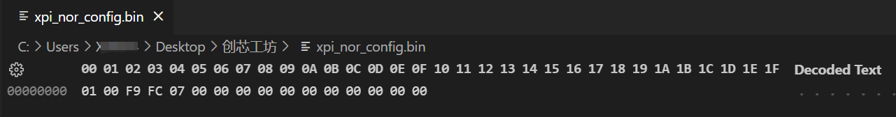
3.1 Flash Configuration Word File
Before writing the working parameters into the chip, you need to first configure the Flash configuration words according to your board's specific settings and generate a .bin file. An example is provided below:
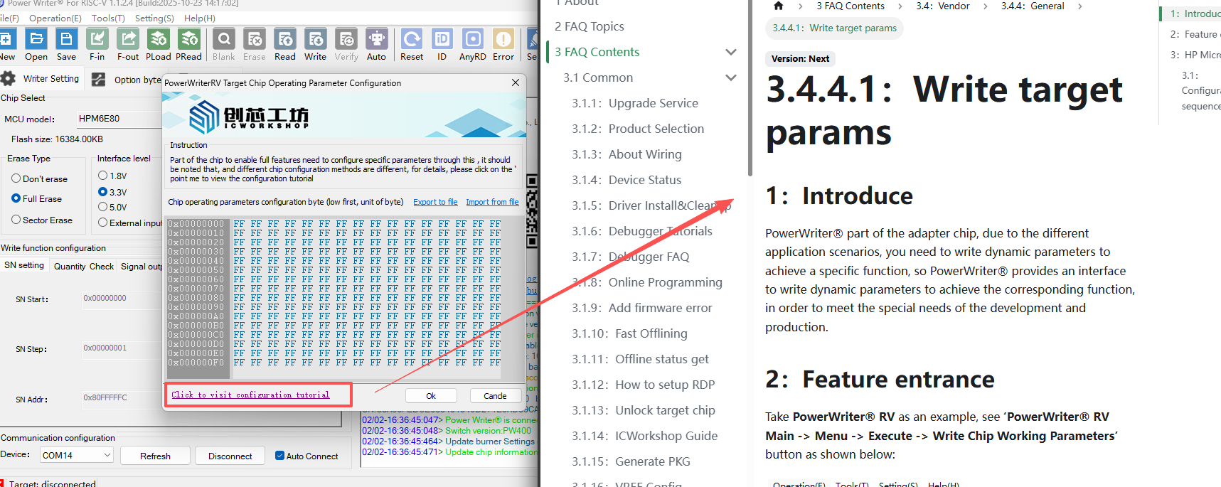
3.2 Writing Parameters to the Chip
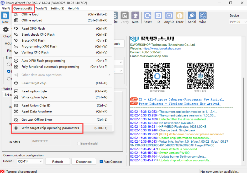
In the PowerWriter® client software, go to the menu bar and select 【Operation】 → 【Write Target Chip Operating Parameters】.
【Import from file】-> 【OK】
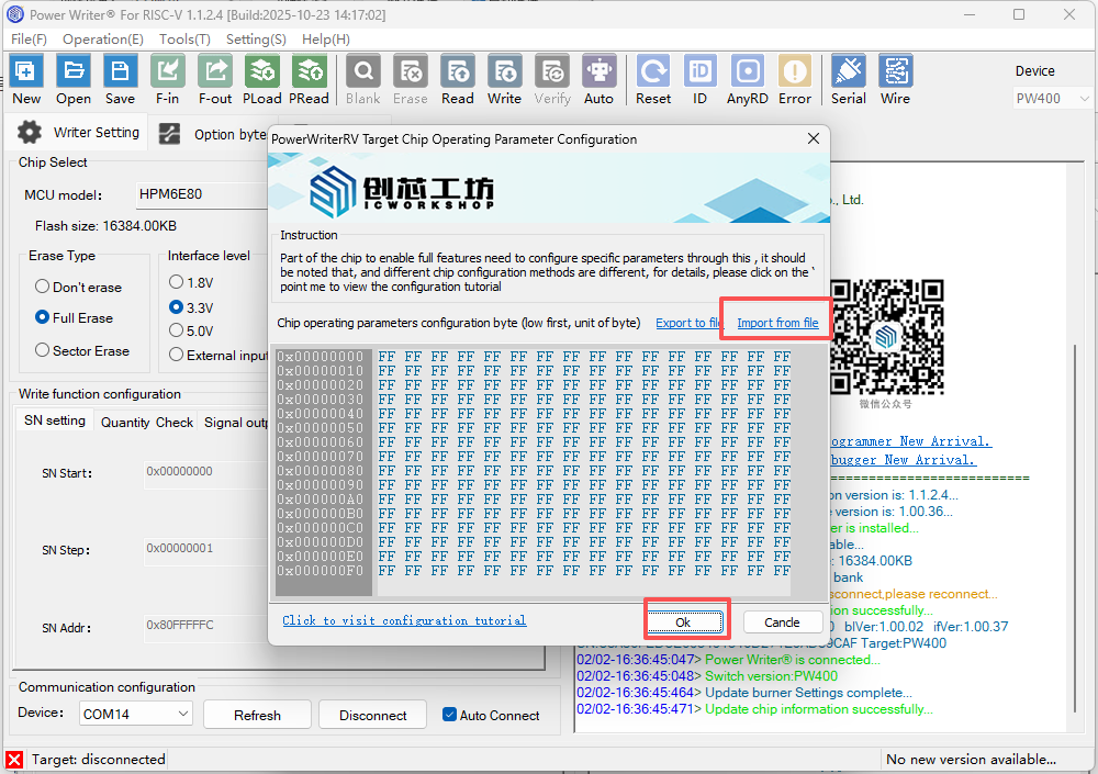
The feature for configuring operating parameters of the target chip supports direct linking to the help documentation.
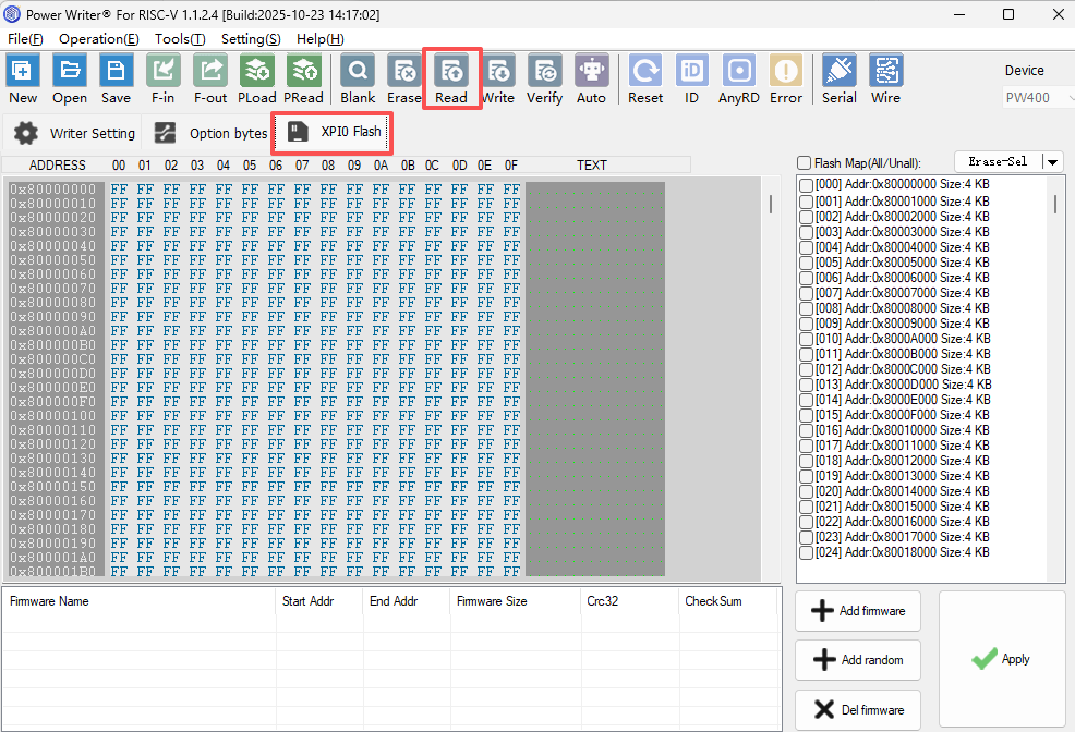
3.3 Reading Flash
After writing the target parameters to the chip, switch to the XPI0 Flash page to perform read operations.
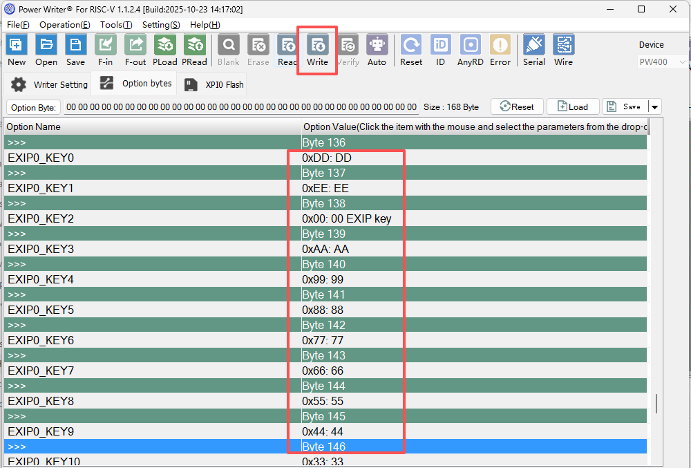
3.4 Writing Option Byte
Switch to the Option Bytes page, configure the OTP (One-Time Programmable) bytes, and then write them to the target chip.