3.1.3:About Wiring
1.PW200/PW300
There are currently two hardware versions of the PW200: one without a screen and another with an OLED display. The image below shows the PW200 equipped with an OLED screen. Compared to the previous PW200, this version only adds the OLED display in terms of hardware—its functionality and usage remain exactly the same.
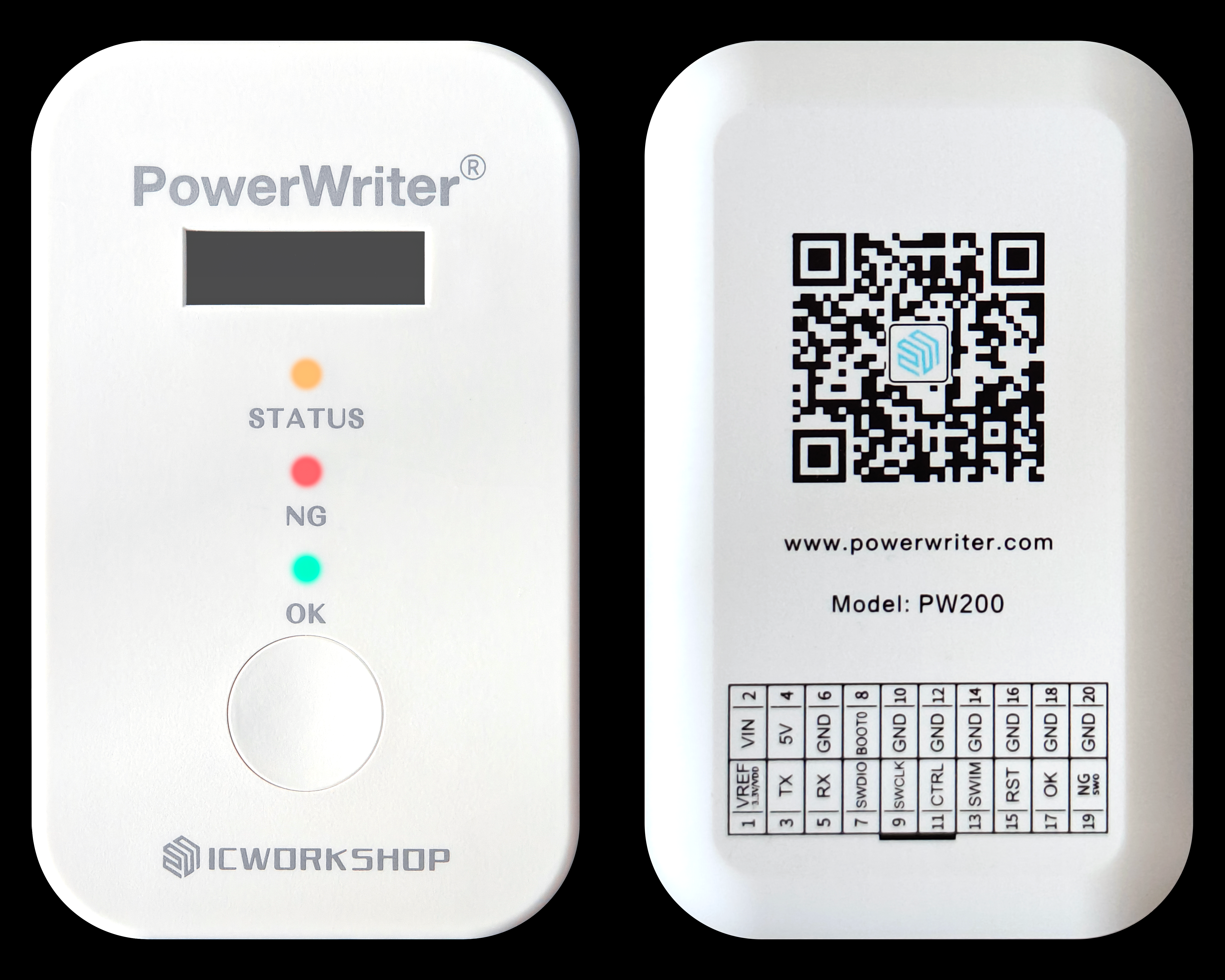
The physical interface diagram of the PW200/PW300 device is shown below:
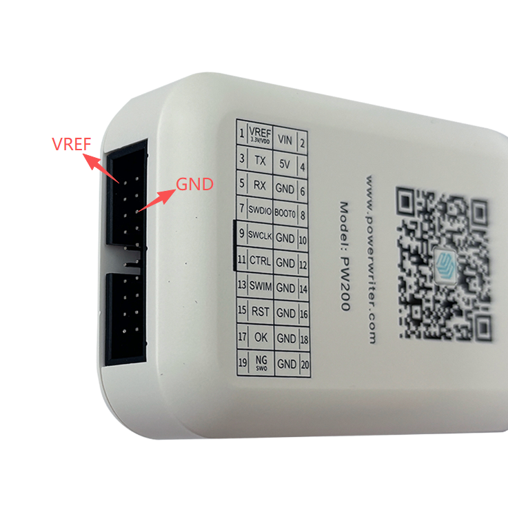
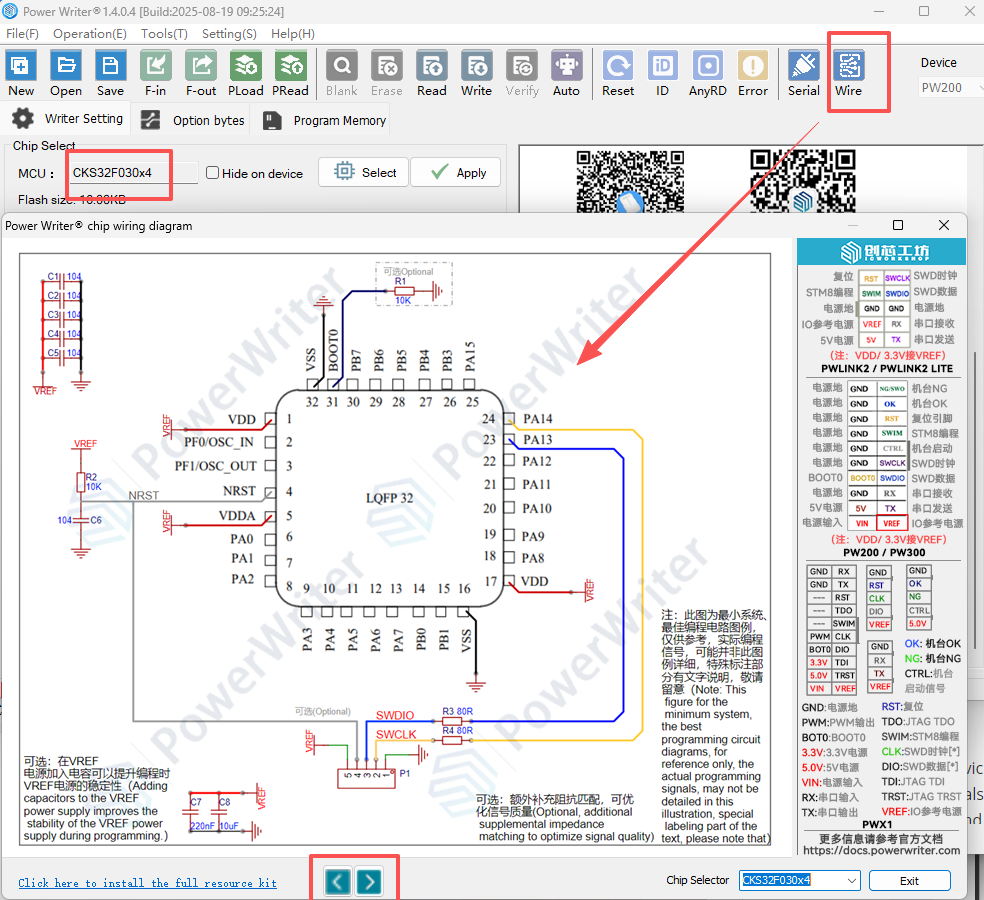
•For ARM-series chips during debugging and programming: Connect the SWD interface of the programmer to the SWD interface of the chip. Wiring: VREF (3.3V/VDD) – VDD GND – GND SWDIO – SWDIO SWCLK – SWCLK •For STM8-series chips: Connect the SWIM interface of the programmer to the SWIM interface of the chip. Note: Debugging STM8-series chips is not supported. Wiring: VREF (3.3V/VDD) – VDD GND – GND SWIM – SWIM RST – RST •For chips programmed via UART (e.g., N32S032): Connect the UART pins. Wiring: VREF (3.3V/VDD) – VDD GND – GND RX – TX TX – RX The PowerWriter® client software provides wiring diagrams for all supported chip models and packages. Click 【Wiring Diagram】 to view. Below is an example for a specific chip:
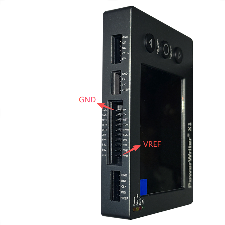
2.PWX1
The hardware version of PWX1 currently includes V1.0 and V1.1. There is a minor difference between the two versions: the positions of the USB-D and USB-H interfaces have been swapped.


The physical interface diagram of the PWX1 with hardware versionV1.0 is shown as follows.
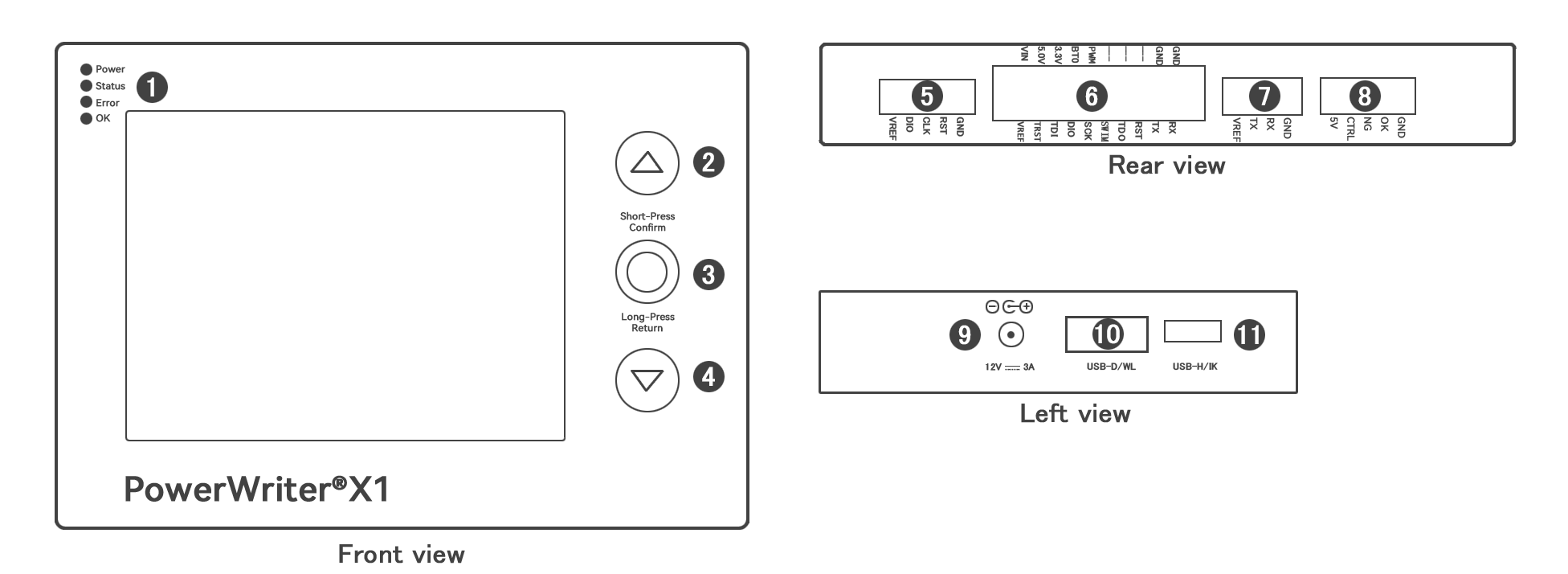
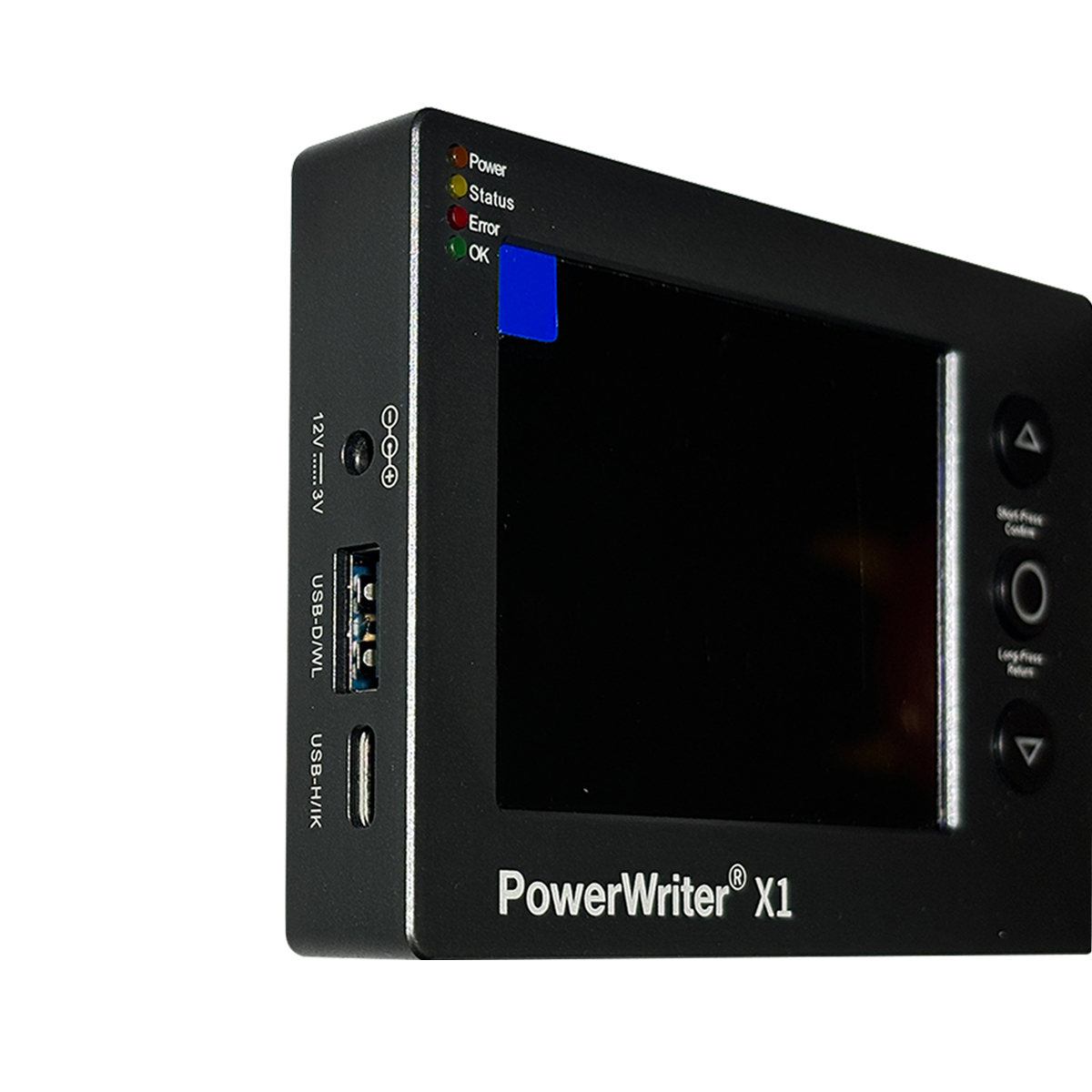
The physical interface diagram of the PWX1 with hardware version V1.1 is shown as follows.


Ports on the conversion board are as follows:
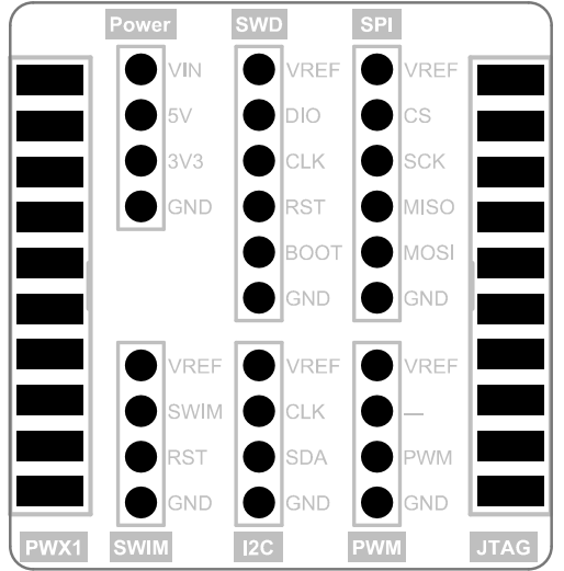
2.1 SWD connection type(ARM )
Connect the device to port 5, or connect the adapter board to port SWD .
2.2 SWIM connection type(STM8)
Connect the SWIM port of the switch board.
2.3 I2C connection type(EEPROM)
Connect the I2C port on the conversion board.
2.4 PWM connection type(wave out)
Connect the PWM interface of the conversion board.
2.5 JTAG connection type(Debugger)
Connect the JTAG port on the switch board.
2.6 SPI connection type(Nor flash)
Connect the SPI interface of the switch board.
2.7 Machine connection mode
See Interface 8.
3.PWLINK2/PWLINK2 Lite
The physical interface diagram of the PWLINK2/PWLINK2 Lite devices is shown below:
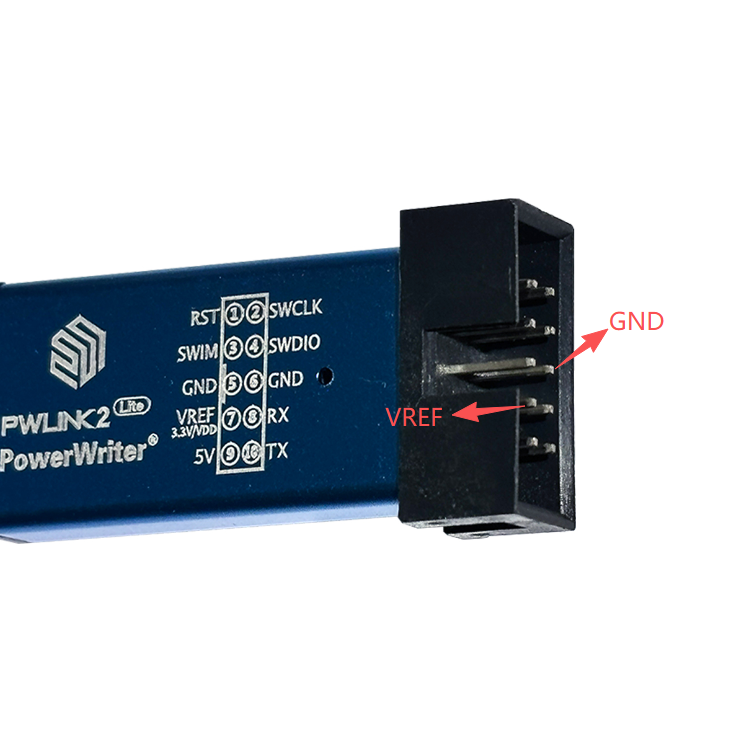
Please note that the PWLINK2/PWLINK2 Lite do not support offline programming features and lack the pins required for standalone operation compared to the PW200/PW300. The definitions of the other pins remain the same. For specific wiring connections, refer to the PW200/PW300 section.
4.PW400
The physical silkscreen diagram of the PW400 device is shown below:
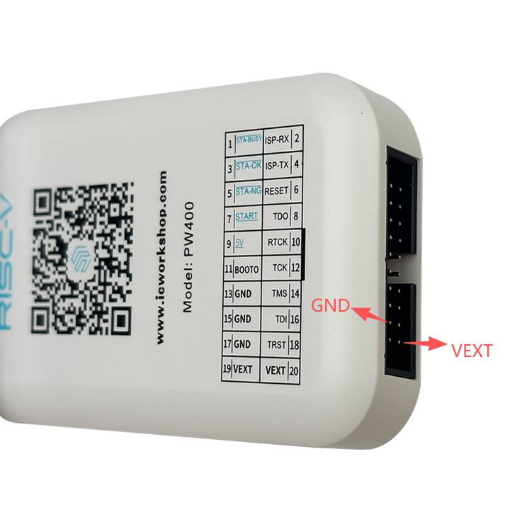
The PW400 primarily supports chips with the RISC-V instruction set.
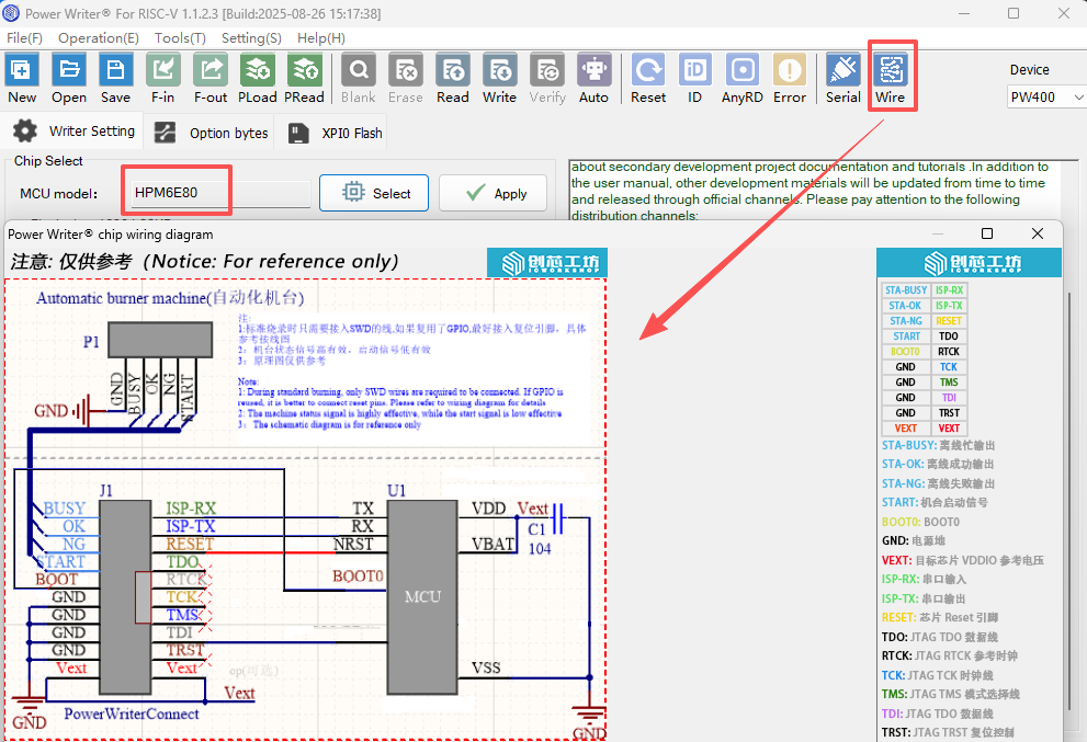
To find out the specific wiring method for programming a particular chip model, please click on 【Wiring Diagram】 in the client software. Below is an example for a specific chip:(Note: The actual example diagram or further specific details about the chip are not provided here but should be referenced in the corresponding section of your documentation.)
- VDD,VEXT, and VREF are powered on at 3.3V by default. You can use the PowerWriter® client to change the power.See How to Set the interface Level .
- The 5V pin can only stabilize the output 5V working voltage and is not controlled by software.
- The VIN pin serves as a power input pin and is not designed to output voltage to external circuits.It is typically used to power the programmer through this pin when it is inconvenient to use a USB cable for power supply.
- If you need information about the other pin functions, please consult the "Hardware Operating Status Description" section.