3.4.7.1: HPM 参数配置
1.芯片说明
先缉半导体的芯片,由于采用外部 FLASH,不同的产品,可能配置外部 Flash 时需要不同的参数,因此,在PowerWriter® 的在线模式下,如果需要使用读取功能读取Flash 数据和单步写入选项字节功能,则需要先对外部Flash 进行参数配置,才能进行操作。
2.配置序列
如需启用读取功能,请参考芯片手册中关于 XPI NOR 配置选项章节内容,或者参考 hpm_sdk-main\boards\hpmxxxx\board.c 中关于Flash 配置的结构定义,以hpm6200evk 为例,结构如下所示:
.\hpm_sdk-main\boards\hpm6200evk\board.c
/**
 * @brief FLASH configuration option definitions:
 * option[0]:
 *    [31:16] 0xfcf9 - FLASH configuration option tag
 *    [15:4]  0 - Reserved
 *    [3:0]   option words (exclude option[0])
 * option[1]:
 *    [31:28] Flash probe type
 *      0 - SFDP SDR / 1 - SFDP DDR
 *      2 - 1-4-4 Read (0xEB, 24-bit address) / 3 - 1-2-2 Read(0xBB, 24-bit address)
 *      4 - HyperFLASH 1.8V / 5 - HyperFLASH 3V
 *      6 - OctaBus DDR (SPI -> OPI DDR)
 *      8 - Xccela DDR (SPI -> OPI DDR)
 *      10 - EcoXiP DDR (SPI -> OPI DDR)
 *    [27:24] Command Pads after Power-on Reset
 *      0 - SPI / 1 - DPI / 2 - QPI / 3 - OPI
 *    [23:20] Command Pads after Configuring FLASH
 *      0 - SPI / 1 - DPI / 2 - QPI / 3 - OPI
 *    [19:16] Quad Enable Sequence (for the device support SFDP 1.0 only)
 *      0 - Not needed
 *      1 - QE bit is at bit 6 in Status Register 1
 *      2 - QE bit is at bit1 in Status Register 2
 *      3 - QE bit is at bit7 in Status Register 2
 *      4 - QE bit is at bit1 in Status Register 2 and should be programmed by 0x31
 *    [15:8] Dummy cycles
 *      0 - Auto-probed / detected / default value
 *      Others - User specified value, for DDR read, the dummy cycles should be 2 * cycles on FLASH datasheet
 *    [7:4] Misc.
 *      0 - Not used
 *      1 - SPI mode
 *      2 - Internal loopback
 *      3 - External DQS
 *    [3:0] Frequency option
 *      1 - 30MHz / 2 - 50MHz / 3 - 66MHz / 4 - 80MHz / 5 - 100MHz / 6 - 120MHz / 7 - 133MHz / 8 - 166MHz
 *
 * option[2] (Effective only if the bit[3:0] in option[0] > 1)
 *    [31:20]  Reserved
 *    [19:16] IO voltage
 *      0 - 3V / 1 - 1.8V
 *    [15:12] Pin group
 *      0 - 1st group / 1 - 2nd group
 *    [11:8] Connection selection
 *      0 - CA_CS0 / 1 - CB_CS0 / 2 - CA_CS0 + CB_CS0 (Two FLASH connected to CA and CB respectively)
 *    [7:0] Drive Strength
 *      0 - Default value
 * option[3] (Effective only if the bit[3:0] in option[0] > 2, required only for the QSPI NOR FLASH that not supports
 *              JESD216)
 *    [31:16] reserved
 *    [15:12] Sector Erase Command Option, not required here
 *    [11:8]  Sector Size Option, not required here
 *    [7:0] Flash Size Option
 *      0 - 4MB / 1 - 8MB / 2 - 16MB
 */
参考如上结构,生成 option[0] ~ option[3] 的 DWORD 字节序列,注意一个 option 是四个字节,一共16字节,填入写入参数对面,点击确定按钮,然后写入操作,如果写入成功,则可以进行在线Flash 的读取操作,写入失败时,将得到对应的提示。
3.操作说明
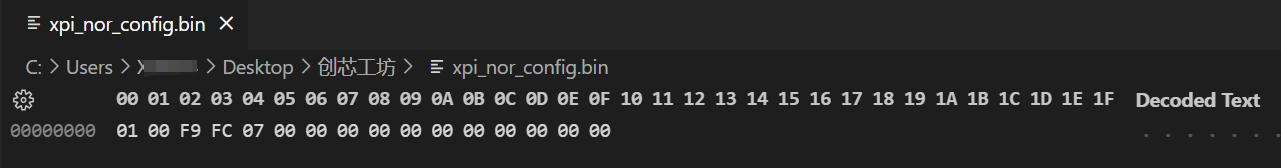
3.1flash配置字文件
在写入芯片的工作参数之前,需要先根据自己板子的配置情况设置flash配置字,生成一个bin文件,如下举例:
3.2写入参数到芯片
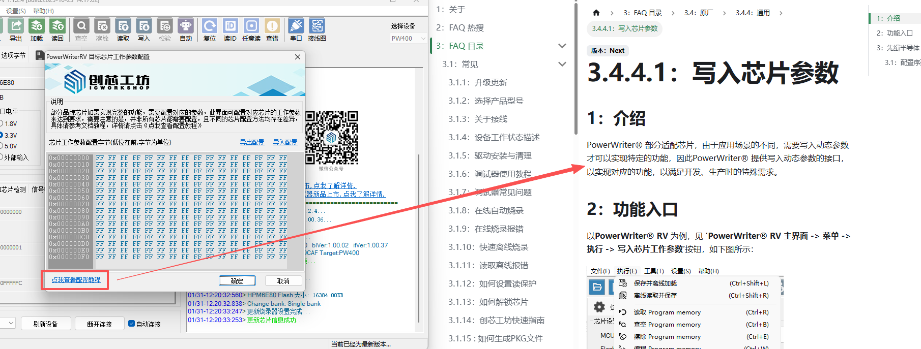
PowerWriter®客户端软件菜单栏【执行】->【写入目标芯片工作参数】
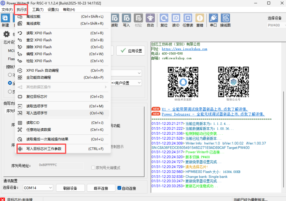
点击【导入配置】-> 添加配置字文件
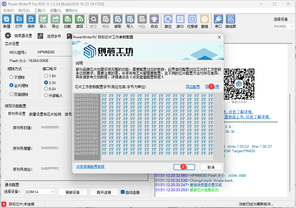
关于目标芯片工作参数配置的功能,支持直接链接到帮助文档。
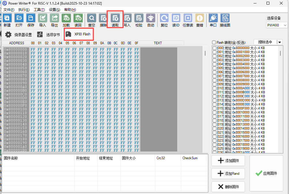
3.3读取flash
写入芯片的目标参数之后,切换搭配XPI0 Flash页面就可以进行读取操作了。
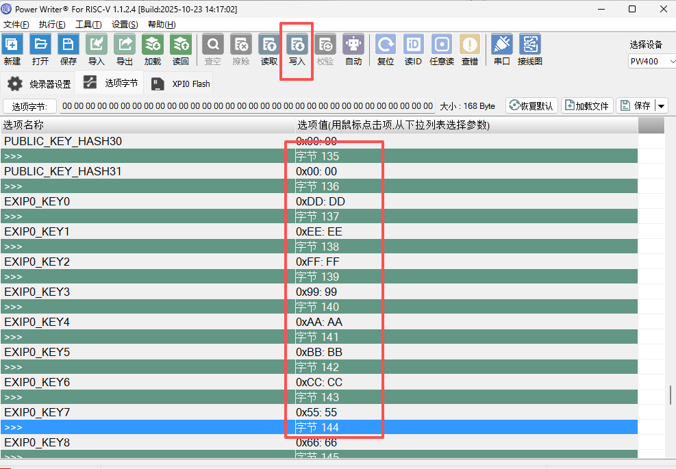
3.4烧写选项字节
切换到选项字节页面,设置OTP字,然后写入到目标芯片中。